CXMT says its fifth-generation DRAM platform has entered mass production, moving the Chinese memory maker’s newest process from development toward repeated factory output. The announcement matters because it could improve chip density, energy efficiency and manufacturing economics for mobile memory. It does not, by itself, prove that CXMT has matched the scale, yields or customer acceptance of the global market leaders.
At a glance
- CXMT announced mass production of its fifth-generation technology platform at the 2026 World Manufacturing Convention.
- The company introduced two 24-gigabit LPDDR5X products and said the platform can produce at least 50% more dies per wafer than its previous generation.
- The next tests are manufacturing yield, customer qualification, reliability and sustained high-volume supply.
What did CXMT announce?
On September 20, 2026, Reuters reported that ChangXin Memory Technologies, better known as CXMT, had put its fifth-generation memory technology platform into mass production. The company also unveiled two 24-gigabit LPDDR5X chips intended for phones and other mobile devices.
CXMT said the new products provide 50% more capacity than its previous generation. It also said the production platform delivers at least 50% more gross dies per wafer. Those are company claims announced at an industry event; real-world competitiveness will depend on how many usable chips each wafer yields and whether customers approve them for commercial devices.
What is CXMT fifth-generation DRAM?
DRAM is the short-term working memory used by phones, PCs, servers and many other electronic systems. It holds data that a processor needs quickly, but unlike storage, it loses that data when power is removed. LPDDR5X is a low-power form designed for mobile products where speed and battery efficiency both matter.
CXMT described a cell-feature spacing of 11.95 nanometres and the use of quadruple patterning. Patterning is a manufacturing technique that repeatedly transfers fine circuit features onto a wafer. Multiple patterning can create smaller features with existing lithography equipment, but it also adds processing steps and makes tight production control important.
The spacing figure should not be treated as a simple equivalent to the marketing “node” labels used for logic processors. Memory geometry, cell design and manufacturing methods are different. The meaningful commercial questions are density, performance, power use, yield and cost.
Why does 50% more dies per wafer matter?
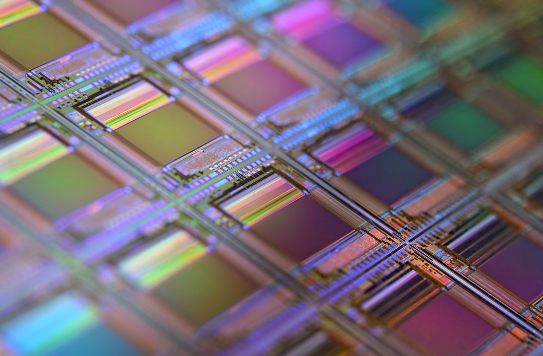
A wafer has a fixed surface area. If each chip occupies less space, a manufacturer can fit more gross dies onto it. In principle, that can reduce the manufacturing cost per chip and increase output from the same factory capacity.
But gross die count is only part of the equation. Defects can make some dies unusable, and advanced processes often need time to reach stable yields. A smaller design that produces many defective chips can be less economical than a larger, mature design. CXMT has not publicly supplied enough independently verified yield data to settle that comparison.
Why it matters
Memory is a strategic part of the semiconductor supply chain, currently dominated globally by Samsung Electronics, SK Hynix and Micron Technology. A viable additional supplier could affect pricing, procurement choices and competition—especially inside China, where policymakers and manufacturers are trying to reduce exposure to foreign technology restrictions.
The announcement also shows why memory competition is not limited to headline-grabbing AI accelerators. Phones, computers and data centres all need large quantities of memory. Improvements in cost, density and power consumption can change a device’s bill of materials even when the central processor stays the same.
For context on how advanced manufacturing affects mobile products, read our explainer on the MediaTek Dimensity 9600 Pro 2nm chip. Our Huawei Atlas 960 SuperPoD analysis explains the separate challenge of building competitive AI systems.
What happens next?
Four signals will determine whether this becomes a major market development: named device customers, independent performance testing, evidence of stable high-volume yields and sustained shipments beyond an initial production run. Customer qualification can take time because memory errors can undermine an entire device.
The safest conclusion today is narrow but significant: CXMT says its newest DRAM platform is no longer merely experimental. Whether it changes the global balance will be decided by production consistency and adoption, not the launch announcement alone.